
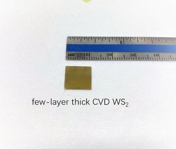
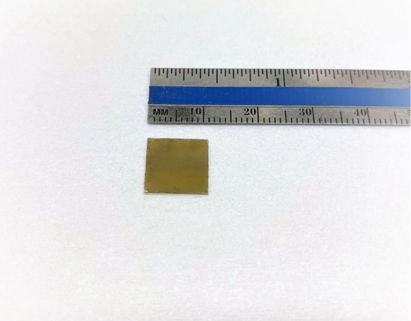
CVD-WS2多层薄膜 1cm*1cm
样品照片:
Ram:
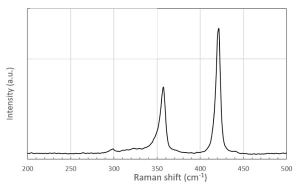
This product contains full area coverage WS2 few-layers that measure ~5 layers in thickness. Sheets are grown through chemical vapor deposition technique onto c-cut double side polished sapphire substrates, but layers c be trsferred onto other substrates by polymer assisted trsfer technique on demd (please select from the drop down menu). The sample measures 1cm2 in size d the entire sample surface contains few-layer thick WS2 sheet. Grown few-layers are high-crystalline as evidenced by HR-TEM, Ram, EDS, d XRD measurements. Please see the datasets in the product images.
Growth method: Our compy synthesizes these few layers using chemical vapor deposition (CVD) using highest purity (6N) gases d precursors in semiconductor grade facilities to produce crystalline d large domain size samples (1-50um). Other sources typically use MOCVD or sputtering process wherein defects are very large, domain sizes are small (10nm-500nm), d products are non-layered. Our samples are always highly crystallized, high purity, d perfectly layered.
Sample Properties
| Sample size | 1cm x 1cm square shaped |
| Substrate type | (0001) c-cut sapphire |
| Coverage | Full coverage few-layer thick WS2 |
| Electrical properties | Indirect gap semiconductor |
| Crystal structure | Hexagonal Phase |
| Unit cell parameters | a = b = 0.312 nm, c = 1.230 nm, α = β = 90, γ = 120° |
| Production method | Chemical Vapor Deposition (CVD) |
| Characterization methods | Ram, photoluminescence, TEM, EDS |
| 参数信息 | |
|---|---|
| 外观状态: | 固体或粉末 |
| 质量指标: | 95%+ |
| 溶解条件: | 有机溶剂/水 |
| CAS号: | N/A |
| 分子量: | N/A |
| 储存条件: | -20℃避光保存 |
| 储存时间: | 1年 |
| 运输条件: | 室温2周 |
| 生产厂家: | 上海金畔生物科技有限公司 |